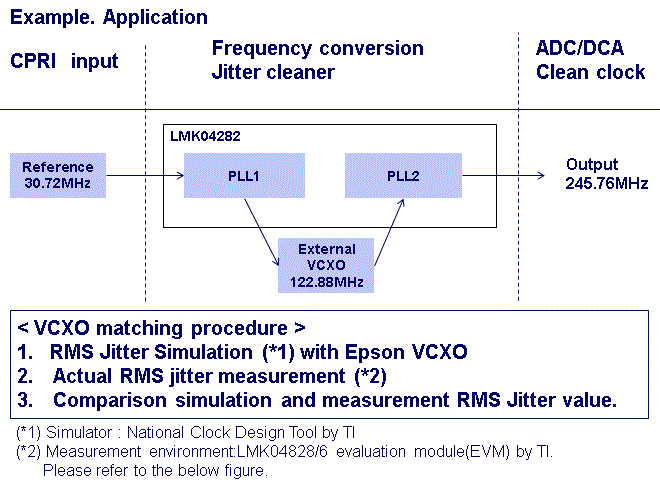
For customers designing Texas Instruments Low Jitter Synthesizer and Jitter Cleaner "LMK04828B"
Epson VCXO matching trial for Texas Instruments Jitter Cleaner LMK04828B
Comparison with Texas Instruments simulator (National Clock Design Tool) and measurement data.
Matching Results
The simulation results matched the measured data well.
As conclusion, VCXOs (VG-4513CA,VG4501CA) have good performance with TI LMK04828B.
For more information, please see the following:
Epson Crystal Product Lineups
| Product | Size [mm] | Applications | Images |
|---|---|---|---|
| VG-4501CA CMOS output | 7.0 x 5.0 x 1.6 | optical networking and base station |

|
| VG-4513CA LV-PECL output | 7.0 x 5.0 x 1.6 | optical networking and base station |
 |
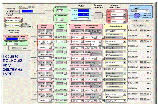
Basic Circuit Block Diagram
Configuration
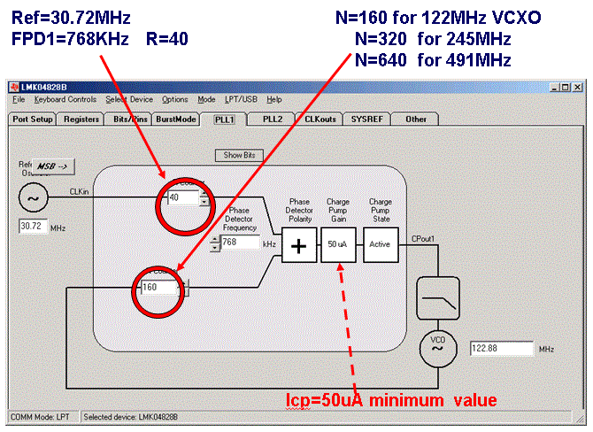
TI LMK04828B Jitter Cleaner(Dual PLL typ.)
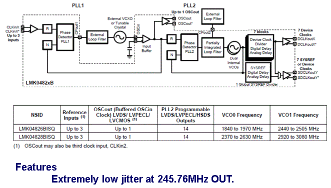
LMK04828B Configuration PLL1
VCXO parameter (measured data)
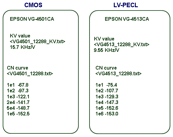
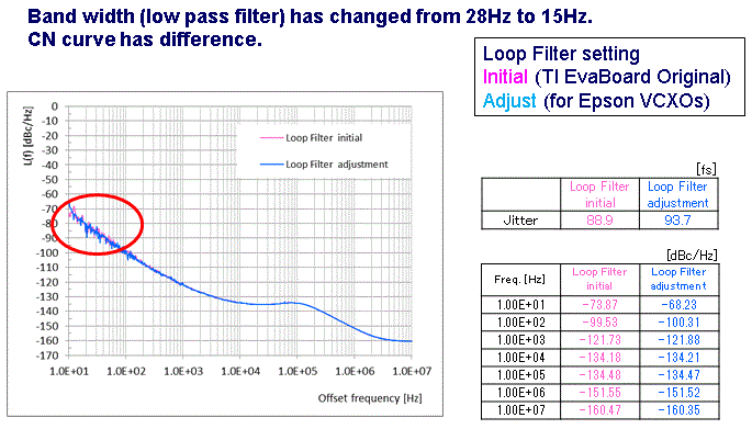
PLL1 Loop Filter - before adjustment (original Value)
| VCXO frequency | VG-4501CA 122 MHz |
VG-4513CA 122 MHz |
|---|---|---|
| KV | 15.7 kHz/V | 9.55 kHz/V |
| lcp | 15.7 kHz/V | 9.55 kHz/V |
| LOOP BW | 40.564 Hz | 28.265 Hz |
| Phase Margin | 40.673 degrees | 46.888 degrees |
| Gamma Optimaztion Factor | 5.857 | 2.844 |
| Natural Frequency | 17.851 Hz | 13.922 Hz |
| Damping Factor | 1.487 | 1.16 |
PLL1 Loop Filter adjustment for Epson VCXOs
| Components | VG-4501CA 122.88 MHz CMOS output |
VG-4513CA 122.88 MHz LV-PECL output |
|---|---|---|
| KV | 15.7 kHz/V | 9.55 kHz/V |
| R2_A1 | 10K | 18K |
| C1_A1 | 390 nF | 220 nF |
| C2_A1 | 2700 nF | 1000 nF +470 nF |
| I ChargePump | 100 uA | 100 uA |
| LOOP BW | 14.148 Hz | 15.195 Hz |
| Phase Margin | 50.5 degrees | 50.2 degrees |
LMK04828B Configuration PLL2
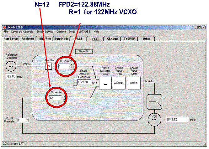
PLL2 Loop Filter
Evaboard default value - no change
| C1_A2 | 0.047 nF | Evaboard original |
| C2_A2 | 3.9 nF | Evaboard original |
| C3 Internal | 10 pF | minimum |
| C4 Internal | 10 pF | minimum |
| R2_A2 | 0.62 Kohm | Evaboard original |
| R3 Internal | 0.2 Kohm | minimum |
| R4 Internal | 0.2 Kohm | minimum |
| I ChargePump | 3200 uA | maximum |
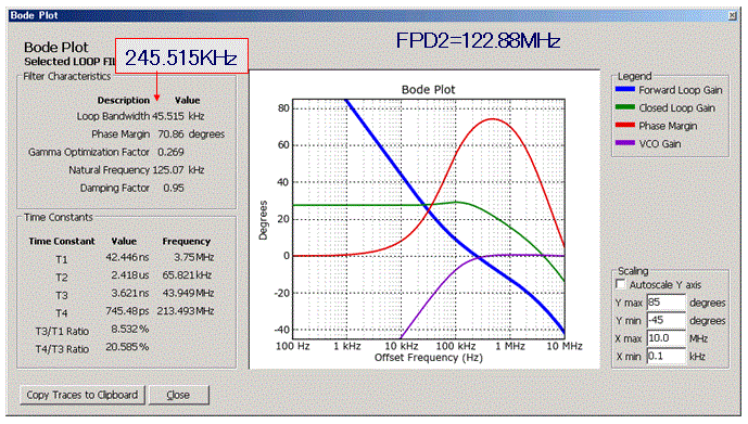
PLL2 Loop Filter Characteristics
| VCXO frequency | 122 MHz R=1 N=8 |
|---|---|
| KV | 18.3734 MHz/V |
| LOOP BW | 245.515 kHz |
| Phase Margin | 70.86 degrees |
| Gamma Optimaztion Factor | 0.269 |
| Natural Frequency | 0.2 Kohm |
| R4 Internal | 125.07 kHz |
| Damping Factor | 0.95 |
PLL2 Bode Plot PFD2=122.88 MHz
Output Setup
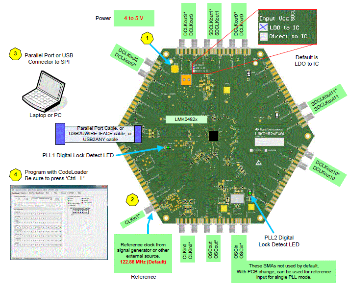
Materials
| Evaluation Board | LMK04828BEVAL | 1 pcs |
|---|---|---|
| OCXO | OX-6501GG | 30.72 MHz |
| ESC Signal Generator | E4438C | 30.72 MHz FM Noise Mod |
| Power Supply | 5 V | E363A and othwes |
| VCXO1 | VG-4513CA | Epson 122.88/245.76/491.52 MHz |
| VCXO2 | VG4501CA | Epson 122.88 MHz CMOS |
| PC | Thinkpad X32 | WindowsXP |
| Chip Control Application | CodeLoader4 | Version4.7.5 Part File v1.8.5 |
| Simulator | NCDT Clock Disign Tool | Version1.3.5 |
Simulation Results
CN curve w/VG-4513CA 122 MHz -> 245 MHz OUT
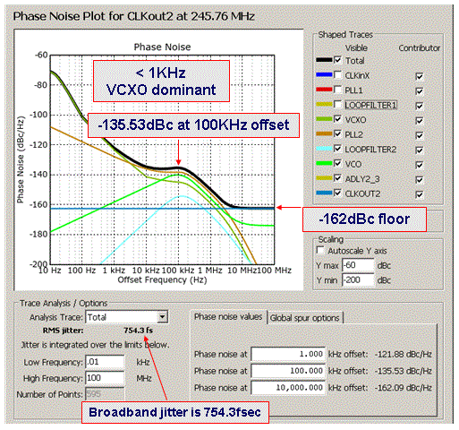
CN curve w/VG-4513CA 245 MHz -> 245 MHz OUT
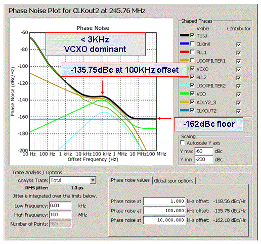
CN curve w/VG-4501CA 122 MHz -> 245 MHz OUT
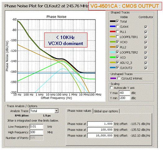
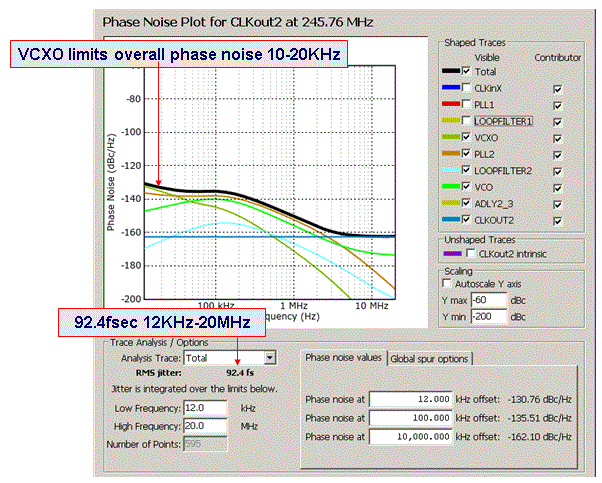
Phase jitter w/VG-4501CA 122 MHz -> 245 MHz OUT
Comparison Results - Simulator vs Measurement
Phase jitter results
| VCXO | simulation | Measured value | Difference |
|---|---|---|---|
| VG-4513CA 122.88 MHz LV-PECL |
91.9 fsec | 93.7 fsec | +1.8 fsec |
| VG-4501CA 122.88 MHz CMOS |
92.4 fsec | 92.1 fsec | -0.3 fsec |
PLL OUT 245.76 MHz / VG-4513CA 122.88 MHz