Glossary
A-N
AT crystal unit, AT cut crystal unit
This is a crystal unit that has a crystal chip that was cut at the "AT cut" angle from the quartz crystal crystallographic axis. This is one of the most widely used types of crystal units, which covers the Megahertz (MHz) band. Since this type of unit has frequency - temperature characteristics for cubic functions with inflection point near room temperature, it has excellent temperature characteristics.
Reference : Frequency versus temperature characteristics
Absolute maximum rating
Absolute maximum ratings provide for items and ranges of values to prevent damage of the crystal device or critical changes in characteristics.
APR (Absolute Pull Range)
The range of frequencies that can be controlled from the nominal frequency value. In other words, APR = Frequency Control Range - Frequency Deviation (Frequency Tolerance).
Accumulated jitter
A type of jitter defined in specification. See "jitter".
Reference : Jitter
Allowance of oscillation
This allowance is expressed as a ratio between a crystal oscillation circuit's negative resistance and a crystal unit's CI value. It is a parameter that indicates the quality of the oscillation characteristics.
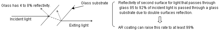
Anti-reflection coating
It is a thin film deposited on the surface of an optical component by evaporation to reduce surface reflections. One typical example is a single-layer made of magnesium fluoride (MgF2.) and there are also multi-layered films that further reduce reflectivity.
4 to 8 % of incident light is reflected on a glass.
Baud rate
The baud rate is the signal volume transferred per second. Usually, this is expressed as bits per second (bps).
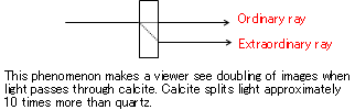
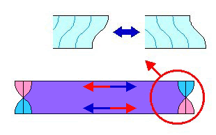
Birefringence
It is a phenomenon in which an incident light beam inputting into a crystal or anisotropic material splits into two light beams of which oscillation is orthogonal each other.
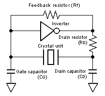
CD
This is the symbol for drain capacitance. See "crystal oscillation circuit".
Reference : Crystal oscillation circuit
CG
This is the symbol for gate capacitance. See "crystal oscillation circuit".
Reference : Crystal oscillation circuit
CI
Abbreviation for "Crystal Impedance". See "equivalent series resistance".
Reference : Equivalent circuit of crystal unit
CL
This is the symbol for load capacitance. See "load capacitance".
Reference : Load capacitance
CMOS
Abbreviation for "Complementary Metal Oxide Semiconductor", which is a type of LSI structure. This is the main type of LSI used today.
CMOS load
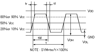
This refers to a circuit that includes a CMOS structure (a type of IC structure) and that has a load circuit connected to the output. The high/low threshold is 50% Vcc.
 |
 |
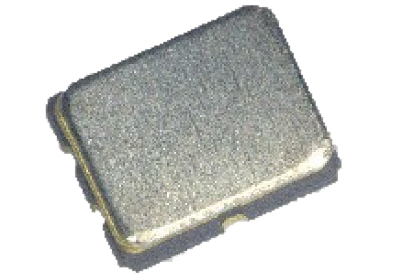
Ceramic package
A ceramic package uses ceramic as part of its package material. To maintain the characteristics of a crystal device over a long period of time, the container must be hermetically sealed. This is why metal materials have been used in the past for packages. Today, ceramic materials are used for compact SMD products.
 |
 |
 |
| Example of ceramic package product | Structure of ceramic package product | |
Clock Oscillator
A clock oscillator is a type of crystal oscillator that provides the square wave pulse required by computers and other digital equipment. Although a clock oscillator has the same configuration as a crystal oscillator that generates accurate frequencies, it is used for different applications. Epson offers clock oscillators in SG series.
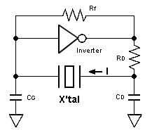
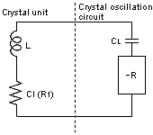
Crystal oscillation circuit
A crystal oscillation circuit is used to drive a crystal unit. The drawing at right shows a crystal oscillation circuit typically used with CMOS ICs.
Reference : Oscillation circuit parameter
Crystal oscillator
A crystal oscillator is a crystal device that is able to output a specified frequency because a crystal oscillator and a crystal oscillation circuit (IC) are incorporated into a single package. A stable frequency can be obtained because matching adjustments between the crystal unit and crystal oscillation circuit has been completed. Epson recommends using crystal oscillators rather than crystal units.
Crystal unit
This is a crystal device that a crystal chip is enclosed in a package. Crystal units can be classified into tuning fork crystal units, AT crystal units, or SAW resonators, depending on the type of crystal chip used.
Reference : Tuning fork crystal unitAT crystal unit
Deterministic Jitter
A type of jitter defined in specification. See "jitter".
Reference : Jitter
Divider Dividing circuit
This circuit is used to generate a low-frequency clock from a reference clock frequency. The division rate is usually 1/n (where n is an integer).
Drain resistor
This is an element in a crystal oscillation circuit. See "crystal oscillation circuit".
Reference : Crystal oscillation circuit
Drive level (Level of drive)
This refers to the power or oscillation output level required to operate (drive) a crystal unit. The drive level is expressed by the following formula. Drive level P = I2 x Re Where I is the current flowing to the crystal unit, Re is the crystal unit's effective resistance, and Re = R1 x (1+ C0/CL) (CL: load capacitance)
 |
 |
| Crystal oscillation circuit | Equivalent circuit of crystal unit |
DTCXO (Digital Temperature Compensated X'tal(crystal) Oscillator)
DTCXO stands for Digital Temperature Compensated X'tal(crystal) Oscillator, and is a oscillator with digitally temperature compencated circuit such as Epson's high accuracy RTC.
Effective resistance
The equivalent resistance of a quartz crystal under load, which can be calculated as Re by the following equation: Re=R1(1+Co/CL)²
EMI noise
This noise is emitted as electric waves from crystal oscillation circuits and peripheral circuits. The higher-frequency components of the oscillation frequency range is the main components of the electric wave interference noise.
Electrode
Electrodes exist as the metal layers that has been formed on a crystal chip surface in order to drive a crystal chip and produce a drive output. Usually, metals such as gold, silver, or chrome are used due to their anti-corrosive properties, their affinity with crystal materials, and also cost benefits.
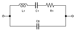
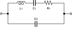
Equivalent circuit of crystal unit
An example of an equivalent circuit for a crystal unit is shown at right. In this example, electrical circuits replace the crystal unit's resonance operation mode.
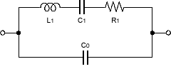 |
| Equivalent circuit of crystal unit |
Feedback resistor
This is a component in a crystal oscillation circuit. See "crystal oscillation circuit".
Reference : Crystal oscillation circuit
Flexure vibration
Flexure vibration is a vibration mode (style) of crystal chips, in which flexure motion of the vibrating piece is used as the oscillation source, such as in tuning fork crystal chips. This type is suited for low-frequency crystal devices.
Flexure vibration
Reference : Tuning fork crystal unit
Frequency
The frequency is the density of cycles (waves) per unit of time (one second). The relation between frequency (f) and cycle time (t) is f (Hz) = 1/t (s).
Frequency control range
In a voltage controlled crystal oscillator, the range of frequencies that can be controlled by an input to the Vc pin. Here, APR (absolute pull range) refers to the range of frequencies that can be controlled from the nominal frequency value. In other words, APR = frequency control range - frequency deviation (frequency tolerance).
Frequency pulling range
This is the range in which the frequency can be changed by input to the Vc pin in a voltage controlled crystal oscillator.
Reference : Voltage controlled crystal oscillator
Frequency stability (Frequency tolerance)
Frequency stability refers to defining a crystal oscillator's specified tolerance ranges (including the tolerances for frequency temperature characteristics and frequency-voltage characteristics) (Δ f) for specified output frequency (fo) within the specified temperature conditions and operating voltage range. It is usually expressed as a ratio (Δ f/fo).
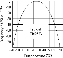
Frequency versus temperature characteristics
This refers to the variation in frequency due to ambient temperature changes, relative to the reference frequency at +25 ℃. The frequency temperature characteristics are generally expressed by the following approximate formula.
 |
 |
 |
| Example of tuning fork crystal unit's frequency temperature characteristics | Example of AT crystal unit's frequency temperature characteristics | Example of SAW resonator's frequency temperature characteristics |
- Tuning fork crystal unit. SAW Resonator.
f_tem=B (Ti-θX)2 θX:specified temperature - AT crystal unit.
f_tem=α (θX-25)+β (θX-25)2+γ (θX-25)3 - SAW resonator, SAW oscillator:Δf/f = a(θT-θX)2
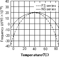
Seiko Epson offers SAW resonators/oscillators with a normal level of frequency temperature characteristics as well as those with a half coefficient of frequency temperature characteristics (New SAW: NS-32R, EG-2121, EG-2102).
Frequency tolerance
The frequency tolerance, when applied to the frequency specification of the crystal units and SAW resonators, indicates the deviation(Δf)of the actual frequency (measured value) from the nominal frequency value (f) within the +25℃ ambient temperature and specified conditions. It is usually expressed as a ratio (Δf/f)
Reference : Frequency stability
Frequency voltage characteristics
Using the output frequency at the central value of the operating voltage range as a reference, frequency voltage characteristics describe variation in output frequency. Variation in frequency due to variation in voltage can be caused by changes in crystal strain or changes in the internal constants of the IC that is built in a crystal oscillation circuit or real time clock. The IC generally plays the greatest role in causing this variation.
Fundamental mode
This is the first (fundamental) vibration order among the vibration orders excited by an AT vibration mode. The stable oscillation provided by the fundamental order makes it easier to design a crystal oscillation circuit than if a higher (overtone) oscillation order were used.
 |
 |
| Fundamental mode | (Reference)Third overtone mode |
Reference : Thickness shear vibrationOvertone mode
GND
This is the symbol for a signal's reference potential (0 V).
Gate Capacitor
This is a component in a crystal oscillation circuit. See "crystal oscillation circuit".
Reference : Crystal oscillation circuit
Half wave plate
It gives a light path difference of a half wavelength (phase difference δ = 180° + N x 360°, N is an integer ) to two linearly polarized light (parallel and perpendicular light components) when light passes through the half-waveplate. It rotates the plane of polarization by the required angle.
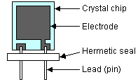
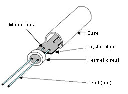
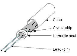
Hermetic seal
A hermetic seal is part of a metal can package that allows a lead (pin) to protrude from the package while maintaining the vacuum condition and insulation of the output signal.

Structure diagram of crystal unit
High frequency
The high frequency band is in the megahertz (MHz) section of the frequency spectrum.
Hz
This is the symbol for Hertz, a unit of measure for frequency. 103 Hz = 1 kHz (kilohertz), 106 Hz = 1 MHz (megahertz), and 109 Hz = 1 GHz (gigahertz).
I²C-BUS interface
This is a type of serial interface, originally proposed by Royal NXP semiconductors.
Initial tolerance
This refers to initial deviation (δf) between the actual frequency (measured value) and the rated value (f) at an ambient temperature of +25 ℃. This differential is expressed as a ratio (δf/f).
Reference : Frequency tolerance
Insulation resistance
This is the resistance value between the leads and between the leads and the case.
Inverter
An inverter is a circuit element that outputs a signal whose high/low status is the reverse of the corresponding input signal. Inverters are used in crystal oscillation circuit to help generate crystal oscillation.
Reference : Crystal oscillation circuit
Jitter
Time domain deviation or fluctuation that occurs in a signal waveform.
-
Period jitter (peak to peak)
Deviation or fluctuation in the length of one cycle of a signal; peak-to-peak jitter is the difference between the maximum and minimum cycle lengths of a signal. -
Cycle to Cycle Jitter
Cycle to cycle jitter: The shift or fluctuation that occurs in the difference between adjacent single cycles of a signal. The absolute value of the maximum cycle difference is sometimes referred to as Peak to Peak, and the standard deviation of the cycle difference distribution is sometimes referred to as RMS. Cycle to Cycle Jitter = T1 -T2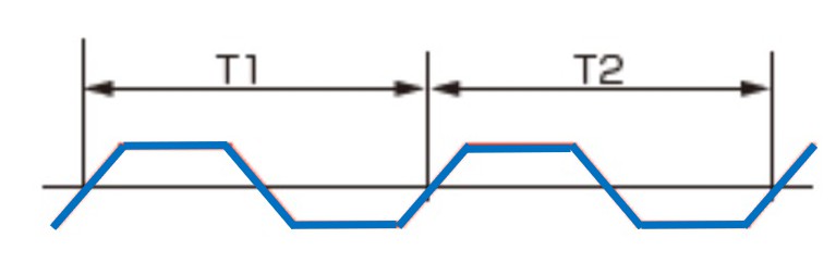
-
Random jitter
Jitter caused by thermal noise or flicker noise. The distribution of jitter shows a normal distribution, and the standard deviation of the distribution is used as the jitter value. -
Deterministic Jitter
Jitter induced by circuit design, electromagnetic induction, and external environment. It is characterized by being finite and predictable (deterministic). In the presence of this jitter, the distribution of jitter appears as multiple overlapping normal distributions (random jitter), and the difference between the maximum and minimum of the median of these normal distributions is the jitter value.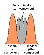
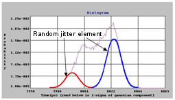
Random jitter and deterministic jitter Example of random jitter -
Total Jitter (TJ)
The maximum amount of jitter that can occur with a given probability, calculated as TJ = DJ + n x RJ, where DJ is a finite value for deterministic jitter, but RJ is normally distributed, so the possible values are infinite. Therefore, the probability of error (BER) is set for TJ, and the value of n is determined according to that probability. n ≈ 14 for BER = 10^-12. -
Phase jitter
Jitter derived from phase noise. Phase noise is frequency instability expressed in the frequency domain, and phase jitter is obtained by integrating this and converting it to the time domain.
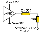
LV-DS
Abbreviation for Low Voltage Differential Signaling. This type of circuit is used for serial transfers of data via low-amplitude differential signals. Since they can be applied for high frequencies.
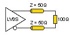 |
 |
| LVDS output definition | Output voltage level comparison |
Lid
This refers to the lid on a ceramic package. The lid can be made of metal, ceramic, glass, or other material, and various lid sealing methods can be used.
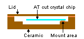
Structure of ceramic package
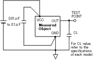
Load capacitance
This is a crystal oscillation circuit's actual capacitance (series equivalent electrostatic capacitance) from the perspective of the crystal unit's two terminals. The oscillation output frequency is determined based on this capacitance. (See CL in the relevant figure at right).
 |
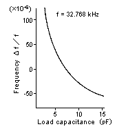 |
| Relation be tween crystal unit and crystal oscillation circuit | Tuning fork crystal unit's load capacitance-frequency characteristics |
Long term jitter
This refers to accumulated jitter. See "jitter".
Reference : Jitter
Maximum drive level
This is the highest drive level at which the crystal unit can operate normally. When a current or charge exceeding this level is applied, degradation of characteristics or physical damage may occur. Special caution is required for tuning fork crystal units.
Maximum supply voltage
This is the maximum rated value for the voltage supplied to a power supply pin. If a voltage exceeding this value is applied, degradation of characteristics or physical damage may occur.
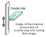
Mechanical processing
This is defined as the use of mechanical methods to create a shape. For crystal devices, mechanical processing has long been used to create tuning fork shapes from crystals. Note with caution that these products differ in terms of dimensions and characteristics from later products that have been fabricated using photolithography processing.
Reference : Photolithography processing
Motional capacitance
The equivalent electrostatic capacitance component in a crystal unit at a series resonance frequency, motional capacitance is equivalent to strain energy. This capacitance is indicated as C1 in the equivalent circuit diagram at right.

Equivalent circuit diagram
Motional resistance
This corresponds to internal equivalent resistance component in crystal oscillator, and is equivalent to the oscillation loss. This can be regarded as a reference for the ease of oscillation. This is also called equivalent serial resistance, and is shown as R1 in the equivalent circuit diagram at right.

Crystal unit's equivalent circuit
Mounting
This refers to the mechanical fixation and getting electrical connection of a crystal chip into a package. Generally, the end of the crystal chip that is minimum impact for vibration is chosen as a fixation area, but since the mechanical strength (adhesion area) conflicts with the crystal chip's characteristics, various fastening methods, adhesives, and structures have been developed recently for small packages.
 |
 |
| Structure of AT crystal unit | Mounting of tuning tork crystal chip |
Negative resistance
This is the resistance value of the crystal oscillation circuit, from the perspective of the crystal unit. As such, it is one of the parameters that indicate the oscillation characteristics of the crystal oscillation circuit. It is called "negative" resistance because energy is generated rather than consumed.

Relation between crystal unit
and crystal oscllation circuit
Nominal frequency
The nominal frequency is the oscillation frequency of a crystal unit with a specified load circuit. Frequency variation of the oscillation depends on the amount of load applied to the crystal oscillation circuit, so "nominal" is attached as an adjective to indicate the oscillation frequency of a crystal unit with a specified load circuit.
O-R
OCXO
Abbreviation for Oven Controlled X'tal (crystal) Oscillator. This type of crystal oscillator is equipped with a small constant-temperature oven in which crystal devices are set in order to provide more stability. With TCXOs, temperature changes are compensated to suppress frequency variation, while with OCXOs frequency drift is suppressed by preventing temperature change in kept at high temperature. Accordingly, OCXOs are used for equipment such as measuring systems and base station communications equipment, which require more high frequency stability than is possible with TCXOs.
Operating temperature range
This is the temperature range within which the specifications (parameter values) of crystal device can be guaranteed.
Operating voltage (Supply voltage)
This is the voltage applied to the VDD/VCC pins, defined as the voltage needed for continuous operation that meets the electrical characteristics.
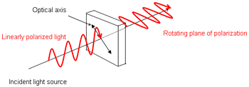
Optic axis
The axis along the direction in which birefringence does not occur (light ray separation does not occur) in a birefringent crystal. This is the Z-axis that runs through the crystal's apex in a quartz.
Oscillation circuit parameter
These are the constants for elements that comprise a crystal oscillation circuit. The parameters differ according to the type of crystal unit, its frequency, and the type of IC being used.
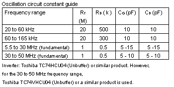 |
 |
| Crystal oscillation circuit |
Reference : Crystal oscillation circuit
Oscillation start-up time
This is the time between when the power supply voltage has reached minimum operating voltage after power-on and when the crystal oscillator starts and reaches stable oscillation.
Output enable
The output enable pin sets stop mode for output while enabling internal circuit operations to continue. It is implemented on a real time clock module or crystal oscillator for use while the system is in stop mode, so as to help reduce the system's power consumption.
Output fall time
This refers to the time (waveform's fall time) required for the transition of output waveform from high voltage (high level) to low voltage (low level). In the figure at right, this time is tf.
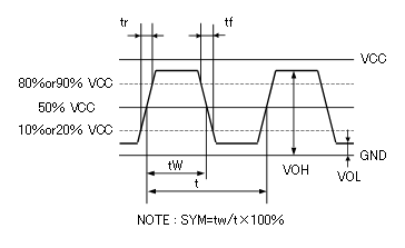 |
 |
| CMOS load output wave form | TTL load output wave form |
Reference : Output rise time
Output frequency
The output frequency is the frequency output from a crystal oscillation circuit or crystal oscillator.
Output load
This is the load applied to CMOS or TTL circuits connected to an output.
Output rise time
This refers to the time (waveform's rise time) required for the transition of output waveform from low voltage (low level) to high voltage (high level). In the figure at right, this time is tf.
 |
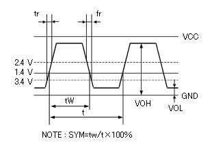 |
| CMOS load output wave form | TTL load output wave form |
Reference : Output fall time
Overtone mode
An overtone mode is a higher vibration order related (as an odd-numbered multiple) to the fundamental vibration order. Each crystal unit has an overtone order in addition to its fundamental order. The overtone order is used to achieve high frequency, which is difficult to be attained with design or fabrication using the fundamental order. Mostly, the third (three times the fundamental) overtone is used.
 |
 |
| (Reference) Fundamental mode | Third overtone mode |
PECL
Abbreviation for Positive Emitter Coupled Logic. This is an I/O level in LSI ICs.
 |
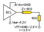 |
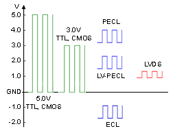 |
| LLV-PECL output definition | ECL output definition | Output voltage level comparison |
PLL
Abbreviation for Phase Locked Loop. This is a circuit or IC that can create any output frequency based on a clock signal having a specified frequency. Recently, these are used with variable reception frequency circuits in TV and radios. Seiko Epson has developed and marketed programmable oscillators that include PLLs.
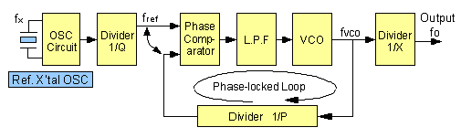
Reference : SG-8000 Series PLL Oscillator
PLL Oscillator
This is a crystal oscillator that includes a PLL circuit. It can also output at over 100 MHz, which is difficult with an ordinary overtone crystal oscillator.
Reference : PLL Programmable Crystal Oscillator
PROM writer
The PROM writer is a programming tool used for programmable crystal oscillators. It is called a PROM writer because it writes frequency data to the internal PROM of programmable crystal oscillators. This is a tool only prepared for use with SG-8000 series. PROM Writer is Seiko Epson registered name.
Reference : SG-Writer Programmable crystal oscillator
Package
A package is a container, such as for a crystal chip, or for crystal chip and IC chip. The package's functions include facilitating board mounting of devices and maintaining an internal vacuum or inert gas in order to optimize the internal crystal's oscillation characteristics.
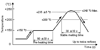
Pb free product
Pb free products are products that all lead has been eliminated from its components and surface-treatment materials. However, Pb free products require a higher soldering temperature than Pb soldered products when mounted.
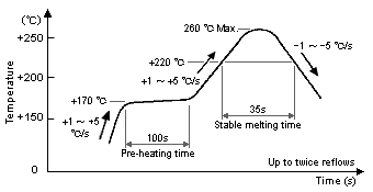
Reflow profile of Pb free products
Reference : Working for EU RoHS/Pb FREE Reflow profile
Period jitter
A type of jitter defined in specification. See "jitter".
Reference : Jitter
Phase noise
This refers to useless energy that is radiated near the oscillation frequency, and that occurs due to the internal and external environmental factors (noise) of a crystal oscillation circuit. Wireless signal transmission errors can occur when this noise value is too high.
Photolithography processing
This type of processing uses chemicals to dissolve a crystal plate or metal layer, usually in order to make a tuning fork crystal shape for a tuning fork crystal chip, or to create electrodes. Before this processing approach was developed, mechanical processing was used, but photolithography processing offers the following advantages.
- This is the same process as is used to fabricate ICs with high dimensional accuracy, so crystal chips can be made very small and very precise, etc.
- Chemical processing enables several hundred tuning fork crystal chips to be made from a single crystal plate, with consistent quality and at low cost.
- Since no strain remains in a crystal chip, the resulting crystal chip provides a stable oscillation frequency for a long time.
Reference : mechanical processing
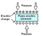
Piezo-electric effect
The piezo-electric effect is the electric charge that is generated in a particular axial direction when pressure is applied in a particular crystal axial direction against a typical crystalline material (such as quartz crystal). By contrast, the mechanical stress that occurs when a charge is applied in the same axial direction is called a reverse piezo-electric effect. Materials that have these properties include monocrystalline materials such as quartz crystal (SiO2), lithium tantalum trioxide(LiTaO3), and lithium niobium trioxide (LiNbO3) , as well as polycrystalline (piezo-ceramic) materials such as barium titanium trioxide(BaTiO3). Each of these materials has its advantages and disadvantages, and quartz crystal is best for stable oscillation.
 |
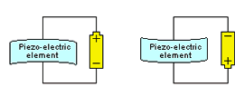 |
| Piezo-electric effect | Reverse piezo-electric effect |
Reference : Piezo-electric element
Piezo-electric element
This refers to any crystal element that has a piezo-electric effect. These crystal elements include monocrystalline elements such as quartz crystal (SiO2), lithium tantalum trioxide (LiTaO3), and lithium niobium trioxide (LiNbO3) elements, as well as polycrystalline ceramic elements.
Reference : Piezo-electric effect
Polishing
This refers to the polishing of crystal plate surfaces. This includes both lapping (with a fine-grained abrasive) and polishing (with a polishing cloth dipped in a polishing substance). These types of surface processing are important for obtaining the desired frequency and to improve the vibration efficiency. In particular, surface accuracy has a very large effect on the characteristics of AT crystal units. Finer surface accuracy is required for higher frequencies.
Programmable crystal oscillator
This indicates the crystal oscillators that include a PLL circuit and can be programmed to output a desired frequency. Being able to program for any output frequency facilitates short-lead-time, small-lot production. A special programming tool is necessary to write frequency data to blank crystal oscillators. Epson programmable crystal oscillators are the SG-8xxx Series, and are programmed by the SG-Writer programming tool.
Reference : Product lineup SG-Writer
Quartz crystal
Quartz crystals are hexagonal mono crystals such as SiO2 crystal. This includes both natural quartz crystal and synthetic quartz crystal. Natural quartz crystals are typically used for ornamental products. They were also used in industrial-use crystal devices until the mid-1960s. Since then, synthetic quartz crystals have been preferred for industrial uses since they have superior quality, relatively few impurities or lattice defects, and can be supplied steadily.
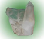 |
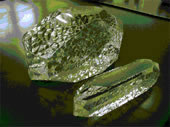 |
| Natural quartz crystal | Synthetic quartz crystal |
RD
This is the symbol for drain resistance. See "crystal oscillation circuit".
Reference : Crystal oscillation circuit
RMS jitter
A type of jitter defined in specification. See "jitter".
Reference : jitter
Random jitter
A type of jitter defined in specification. See "jitter".
Reference : jitter
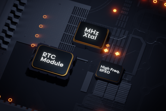
Real time clock
A real time clock is a circuit or IC that generates digital data for times and dates, etc. from a reference clock. Usually, the reference clock is a 32.768 kHz crystal unit.
Reference : Real time clock module
Real time clock module
A real time clock module is a crystal device incorporating into a single package a 32.768 kHz crystal unit and a real time clock IC. This module is used in computers and fax machines and other electronic equipment that requires time management functions. Not only do these modules to eliminate the need to design an oscillation circuit and the need to adjust a timepiece function, they also conserve space on the circuit board.
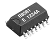
Real time clock module
(RX-8581)
Reference : Real time clock
Reflow
Reflow soldering is one method used to solder electronic devices to circuit boards. This method exposes devices to temperatures over +200 ℃, so reflow soldering must be performed carefully, according to the reflow profile.
Reflow profile
The reflow profile specifies the temperatures and time periods to be set when using the reflow soldering method to mount electronic devices on circuit boards. Failure to follow these specifications can damage the electronic devices, such as by degrading their characteristics.
 |
 |
| Reflow profile soldered product | Pb free soldered product |
Rf
This is the symbol for feedback resistance. See "crystal oscillation circuit".
Reference : Crystal oscillation circuit
S-Z
SAW oscillator
This is a crystal oscillator that houses a SAW resonator chip and IC chip including crystal oscillation circuit in a package. Epson offers SAW oscillators under the EG series. In particular, the EG-2121 and EG-2102 have improved frequency temperature characteristics to one-half their previous levels.
Reference : Frequency versus temperature characteristics
SIP package
Abbreviation for Single In-line Package. This type of package has leads (pins) that protrude from one side, and which are inserted into holes in the circuit board to mount the package.
SIP package
SMD package
This is a general term for any package that is mounted onto the surface of a PCB. SMD is an abbreviation for "Surface Mounted Device". This is one of the newer types of crystal device packages, which typically use ceramic or plastic as the package material.
SOJ package
Abbreviation for Small Outline J-leaded package. In this surface-mount package, the leads (pins) protrude from both sides and the lead ends are bent inward, beneath the package.
SOP package
Abbreviation for Small Outline Package. In this surface-mounted package, the leads (pins) protrude from both sides and the lead ends are bent outward.
Shock resistance
This refers to a crystal device's resistance to shocks. This is evaluated by the amount of change in characteristics (particularly frequency variation) and damages caused by a specified impact. Quartz crystal is a hard and brittle material that fractures easily, so shock resistance is a key characteristic for crystal devices used in mobile products. In the past, an evaluation method was used whereby a certain amount of shock was applied to crystal products by shock testing equipment. Recently, the evaluation method is used wherein a crystal device fixed in a testing tool weighing 100-gram weight is repeatedly dropped from a certain height.
Shunt capacitance
Shunt capacitance is an electrostatic capacitance component that is generated between two electrodes in a crystal oscillator. It is shown as C0 in the equivalent circuit diagram at right.
Equivalent circuit diagram of crystal unit
Standby
The standby is a function which can stop operation of the oscillation circuit and output of a crystal oscillator. This is useful in eliminating power consumption.
Storage temperature
This is the temperature range for maintaining the operability and characteristics of a crystal device that is in storage (not being operated). Storing crystal devices in an environment that is outside this temperature range can cause degradation of characteristics or other damage. Degradation of characteristics can also occur if crystal devices are stored for a long time at temperatures near the upper or lower limits of this range, so Epson recommends that crystal devices be stored under normal room temperature and humidity conditions whenever possible.
Surface Acoustic Wave
Reference : SAW
Synthetic quartz crystal
This refers to quartz crystal that is made artificially, in contrast to naturally occurring quartz crystal. Both types of quartz crystal are used as a material for crystal devices. Whereas naturally occurring quartz crystal contains a lot of impurities and experiences a wide range of quality fluctuation, synthetic quartz crystal contains few impurities, which enables more stable crystal devices to be manufactured. A method called hydrothermal synthesis is used to grow various quartz crystals in specified sizes. The crystals are grown over a period of two months in an autoclave which maintains the processing conditions of a temperature of approximately +400 ℃ and air pressure of 1000 atmospheres.
Synthetic quartz crystal
TCXO
Abbreviation for "Temperature Compensated X'tal (crystal) Oscillator". For further description, see "temperature compensated crystal oscillator".
Reference : Temperature compensated crystal oscillator
Temperature compensated crystal oscillator
This crystal oscillator, called TXCO for short, includes a function for compensating the frequency variation according to the crystal oscillator's temperature. Generally, AT crystal devices have relatively better temperature characteristics. In order to obtain more stable frequencies, the temperature variation is compensated based on signals sent from a temperature sensor. There are two frequency compensation methods: an analog compensation method and a digital compensation method. Epson Applications the TG Series of temperature compensated crystal oscillators.
Reference : TCXO
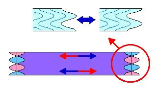
Thickness shear vibration
This is a vibration mode in crystal units. As shown in the drawings at right, in this vibration mode the top and bottom surfaces along the crystal plate's thickness direction move opposite to each other. This mode is used in high-frequency crystal units such as AT crystal units. The frequency f is a function of the crystal chip's thickness T. For the fundamental frequency, f = k/T (k: constant)
 |
 |
| Fundamental mode | Third-order overtone mode |
Reference : AT crystal unit
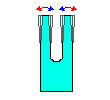
Tuning fork crystal unit
This type of crystal unit uses a tuning fork-shaped crystal chip. Its advantages including being suited for relatively low frequencies and being compact with a vibration plate that can be separated from its supports. See "flexure vibration" for description of the vibration mode.
 |
 |
| Tuning fork crystal chip | aStructure of tuning fork srystal unit |
UV & IR-cut filter coating
It is a multi-layer coating for filtering out both ultraviolet light (light with wavelength of 400 nm or below) and infra-red light (light with wavelength of 650 nm or above). A CCD or CMOS device is sensitive to both ultraviolet and infra-red light. Ultraviolet light casts a bluish tinge on images. This filter coating remove this coloring.
VCC
This is the symbol for a transistor's collector pin (positive power supply pin) and for power supply voltage values. Although the symbol VDD is sometimes used instead, it has a different meaning in the strict sense. See "VDD".
Reference : VDD
VCSO
Abbreviation for "Voltage Controlled SAW Oscillator". For further description, see "Voltage controlled SAW oscillator".
Reference : Voltage controlled SAW oscillator
VCXO
Abbreviation for "Voltage Controlled X'tal (crystal) Oscillator". For further description, see "Voltage controlled crystal oscillator".
Reference : Voltage controlled crystal oscillator
VDD
This is the symbol for a drain power supply pin for MOS type IC or power supply voltage value.
Reference : VCC
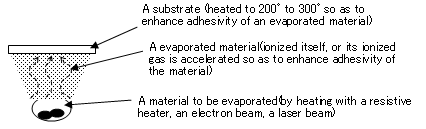
Vacuum deposition
It is a method of forming a thin film on the surface of a substrate by evaporating and depositing metal or dielectric materials in vacuum. The method includes resistance heating vacuum evaporation, E.B. heating vacuum evaporation, sputtering, ion plating, and CVD (Chemical Vapor Deposition)
Voltage controlled SAW oscillator
This type of SAW oscillator (abbreviated as VCSO) includes a function that uses applied voltage to control the oscillation frequency. Generally, it is used for higher frequency bands of at least several hundred MHz. Seiko Epson Applications voltage-controlled SAW oscillators in its EV Series.
Reference : VCSO
Voltage controlled crystal oscillator
This type of crystal oscillator (abbreviated as VCXO) includes a function that uses applied voltage to control the oscillation frequency. Generally, it is used for automatic control systems that include various sensors for controlling the reception frequency. Usually, it also includes a variable capacitor for controlling the oscillation frequency. Seiko Epson Applications voltage-controlled crystal oscillators in its VG series and TCO series.
Reference : VCXO