The History of Epson Crystal Devices
Crystal devices quietly mark the passage of time in everything from TVs to computers and wristwatches. They have grown to become an indispensable fixture in the electronics industry, so much so that the Japanese refer to them as "the salt of industry." As a leading manufacturer of crystal devices, Epson has continuously driven advances in device power savings, miniaturization, and performance. Epson encapsulates its philosophy of innovation with the words "efficient, compact and precise." This approach is embedded in Epson DNA. It is what enables us to continue to develop ever-smaller devices that consume less power yet provide superior performance. This is a brief history of Epson Crystal Devices.
- 1891
- Yoshimura Shokai, the predecessor entity, is established.
- 1938
- Toyo Wireless Telegraph and Telephone, which succeeded Yoshimura Shokai, merged with Meisho Electric to establish Toyo Communication Equipment Co., Ltd.
- 1942
- Daiwa Kogyo, Ltd., the predecessor of Seiko Epson, is established.
- 1943
-
Daini Seikosha, the watch manufacturing division of Hattori Tokeiten, is established.
A factory is established in the city of Suwa, Nagano Prefecture, to escape the air raids of WWII. - 1959
-
The first industrial synthetic crystals to be grown in Japan
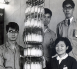 Large, high-quality natural quartz crystals with few impurities were being processed for use, but such crystals were difficult to obtain domestically, because, at the time, quartz was being used worldwide as a military material. Therefore, we set out to independently produce our own large, high-quality synthetic crystals. First, we needed to produce an autoclave and fine-tune it to manufacture high-quality synthetic crystals. More autoclaves were then added to ramp up to mass production. This allowed us to successfully grow the first synthetic crystals in Japan on an industrial scale.
 - Daini Seikosha's Suwa factory and Daiwa Kogyo merge to establish Suwa Seikosha.
- 1969
-
Development of the world's first commercially available quartz wristwatch
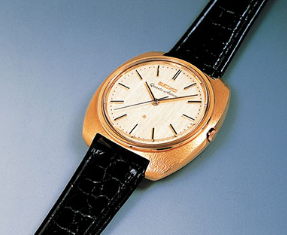
The Seiko Quartz Astron 35SQ, the world's first quartz watch
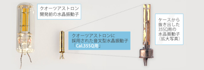
Crystal unit size comparison
(Left) Crystal unit (approx. 50 mm long) that was in practical use prior to the development of the quartz Astron.
(Center) Tuning-fork crystal unit used in the Quartz Astron (4.3 mm in diameter x 18.5 mm in length)Prior to the development of the world's first quartz wristwatch, extremely accurate quartz timepieces existed but were the size of a wall clock and could not be easily transported. What made the world's first quartz wristwatch, the Seiko Quartz Astron 35SQ, practical were its accuracy and small size. Accurate to an astonishing ±0.2 seconds per day, the Astron was achieved by using a combination of crystal unit, watch IC, and ultra-compact stepping motor technology. Creating the watch required miniaturizing the crystal unit. Conventional crystal units were far too large to fit into a wristwatch. This problem was solved by using a new tuning fork-type structure. The tuning fork crystal unit for the 35SQ caliber was 4.3 mm in diameter and 18.5 mm in length. The problem of constant exposure to vibrations and physical shocks when worn on the wrist was solved by modifying the internal structure of the crystal unit.
Development of CMOS ICs for watches begins
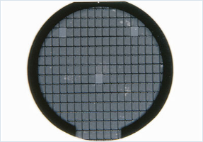 However, even the Quartz Astron was somewhat large. To popularize quartz wristwatches, the wristwatch and its built-in tuning-fork crystal unit had to be smaller, which meant that the crystal unit's vibration frequency had to be increased. Increasing the vibration frequency itself is not difficult, but doing so increases power consumption. It thus became necessary to shrink the size, reduce the power consumption, and improve the durability of the core components, including the IC chip. At the time, however, no domestic manufacturer was producing ICs specifically for quartz watches, so a decision was made to develop CMOS ICs by ourselves and mass-produce them in-house.
 - 1971
-
Advent of a smaller crystal unit that consumes less power
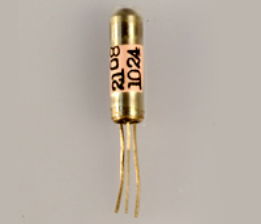
Tuning fork crystal unit for the Cal. 38
We succeeded in developing a smaller tuning-fork crystal unit for the Cal. 38. It vibrated at a frequency of 16.384 kHz and measured 4.3 mm in diameter and 14.7 mm in length. - 1973
-
Crystal unit further miniaturized and 32.768 kHz becomes the de facto standard vibration frequency
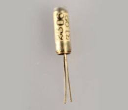
Tuning fork crystal unit for the Cal. 57
We succeeded in developing an even smaller crystal unit for the Cal. 57. With a diameter of 3.9 mm and a length of 10.9 mm, this crystal unit also had a higher vibration frequency: 32.768 kHz. The 32.768 kHz vibration frequency has become the de facto standard vibration frequency for crystal units used in watches today. -
Development of a thin, flat tuning-fork crystal unit for simple mounting
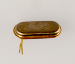
An F-001 flat tuning fork crystal unit
We also introduced a flat, rather than cylindrical, tuning-fork crystal unit. At 5.1 mm x 12.1 mm x 2.4 mm, the F-001 crystal unit was slightly larger than the crystal unit used for the Cal. 57, but it was far easier to assemble (mount) on a printed circuit board populated with other electronic components. Cylindrical crystal units had to be mounted so that they stood vertically on the circuit board, with the metal terminals bent and laid flat on the board. In contrast, the flat type could be mounted simply by inserting it into the board. The F-001 was quickly adopted in affordable small wristwatches and LCD watches, which required electronic circuits to be housed under the LCD panel. -
The world's first wristwatch with a six-digit LCD display
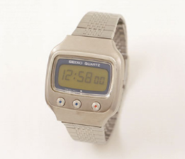
Figure: Seiko Quartz 06LC
Mass production of CMOS ICs for watches, which had been under development since 1969, also began in this year.
These CMOS ICs were used in the Seiko Quartz 06LC, the world's first wristwatch with a six-digit LCD display. - 1975
-
Photolithography for further component downsizing and higher precision
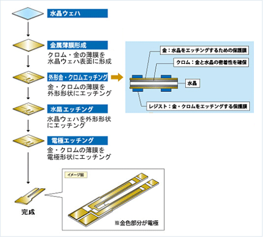
Photolithography process flow of the day
A photolithography process is used to fabricate minute patterns on quartz wafers by exposing a thin layer of metal deposited on the wafer to light and then etching the unwanted areas. It was already an indispensable technology for fabricating integrated circuits (ICs). Photolithography greatly contributed to crystal miniaturization, precision, and production. -
Sales launched of the first tuning-fork crystal units produced using photolithography
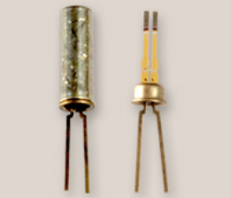
The C-002 was the first crystal unit to be manufactured using photolithography.
The C-002 was the first crystal unit fabricated using photolithography to become commercially available. It measured 2 mm in diameter and 6 mm in length. The vibration frequency was 32.768 kHz. - 1980
-
Sales of crystal oscillators integrating Epson crystals and semiconductors launched
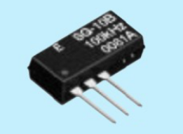 The Fujimi Plant was established to develop and scale up production of semiconductors. In the same year, the company introduced its first crystal oscillator, which combined a tuning-fork crystal unit with a watch IC developed in-house.
 - 1983
-
RTC module with a built-in crystal unit
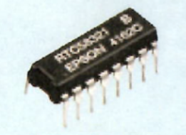 Further integration of crystals with semiconductors resulted in the RTC-58321, a real-time clock module with a built-in crystal unit that went on sale that same year. Since then, we have provided the world with a wide variety of RTC modules by continuing to integrate our crystals and RTC ICs and drive advances in the technology that we originally developed to reduce power consumption and increase the accuracy of our watches.
 - 1983
-
Temperature compensated crystal oscillator (TCXO) used in early cell phones
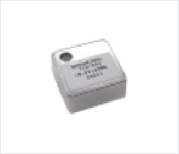 Shoulder phones - the first mobile phones - became a hot topic when they first appeared in the 1980s. As the name implies, they could be slung on a shoulder and carried around, serving as a harbinger for what was to come: the transition from landlines to mobile phones and, eventually, today's smartphones. Since these phones were used outdoors and in a variety of temperature environments, the oscillators used in them needed to maintain frequency stability over a wide temperature range. This need led us to develop and mass-produce our first temperature-compensated crystal oscillator (TCXO), a device with a cubic volume of about 4.0 cc. Epson has been reducing the size of its TCXOs by adopting internal oscillation circuits, temperature compensation circuits, and crystal chips fabricated in a photolithography process. Today, our TCXOs have a cubic volume of 0.003 cc-1/1300 that of our first TCXO.
 - 1984
-
SAW filters launched to market
Monolithic crystal filters (MCFs) were commercially available, but it was difficult to reduce the thickness of quartz substrates with the technology of the day, making MCFs unable to cope with frequencies above about 70 MHz. We then turned our attention to Surface Acoustic Wave (SAW) filters, anticipating that higher frequencies could be handled by narrowing the spacing between inter-digital transducers (IDTs), comb-shaped electrodes fabricated on the surface of quartz substrates. MCF principles were brought to SAW filters. Two SAW resonators are placed adjacent to one another and the acoustic coupling between these two resonators excited two different resonance frequencies: f1 (corresponding to first-order vibration mode) and f2 (corresponding to the second-order vibration mode). These two frequencies are used to realize a filter that functions on the same principle as an MCF. SAW filters were an exciting development within the wireless communication equipment industry because they would make it possible to produce wireless communication devices that were significantly smaller and cheaper.
Photolithography is used for SAW filters to fabricate IDTs in quartz substrates. Researchers realized that they could use this technology to thinly shave material from quartz substrates and increase crystal unit and MCF frequencies. The conventional machining techniques used up to that point could only produce components that could handle up to about 70 MHz, but by chemically shaving only the vibrating portion in the center of the quartz substrate, they were at last able to handle higher frequencies. This manufacturing technique was known as High Frequency Fundamental (HFF) and later came to be used in high-frequency crystal units and other devices. - 1986
-
The first commercial cylinder-type AT crystal units and AT crystal oscillators
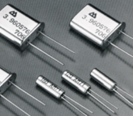
CA-301 cylinder type AT-cut crystal unit (3 mm x 8 mm)
The tuning-fork crystal unit assembly line was diverted to the production and commercialization of cylindrical AT crystal units. The CA-301, measuring 3 mm in diameter and 8 mm in length, was commercialized by purchasing raw quartz crystals and equipment for processing them into quartz wafers. At about the same time, the SG-51 crystal oscillator (clock oscillator), formed by molding an AT-cut crystal unit and oscillation IC together in a plastic mold, was also commercialized.
At 19.8 mm x 6.36 mm x 5.3 mm, both products were a step or two ahead of competing products in terms of miniaturization. - 1987
-
The industry's first surface-mount clock oscillator
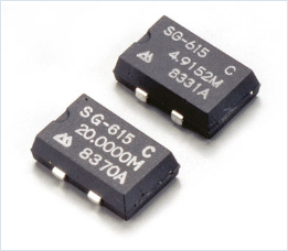
SG-615
This product was created to meet the need for surface mounting on boards, which was becoming popular at the time. Conventional board mounting generally involved drilling holes in a board, inserting the leads of components into the holes, and then soldering them in place. This method had numerous problems. It required drilling through-holes in the boards, which reduced board strength. It also took time, increased component mounting, put constraints on board wiring, and reduced wiring density. In contrast, surface-mount boards allow greater wiring freedom, smaller components, and higher mounting density because components are connected only to the surface. These advances caused surface mount technology to catch on in applications such as office equipment. This also led to the advent of surface mount devices (SMD) such as ICs, but crystal devices in metal packages were still the norm. To change this situation, we began developing crystal device plastic packages and SMDs that capitalized on the mass production technology we had cultivated in semiconductor manufacturing.The resulting SG-615 used thermosetting epoxy resin as the plastic material. A newly developed heat-resistant cylinder AT-cut crystal unit was built into the oscillator to enable it to withstand the same temperature conditions as those for SMD ICs in reflow furnaces used in the surface-mount soldering process. The fundamental output frequency range was approximately 1 MHz to 26 MHz. Overtone oscillation allowed for even higher-order frequency output. The output signal could be varied by providing an output enable function that allowed the output signal to stop and start. In addition, a maximum current consumption of only 25 mA was achieved by taking advantage of our own CMOS ICs. This product pioneered the shift to SMD in the crystal oscillator industry. Once the SG-615 was selected as a control clock for PCs by a major U.S. computer manufacturer, sales of the clock to other PC manufacturers surged. It became the de facto standard and production reached 3 million units a month at its peak.
- 1997
-
Programmable high-frequency crystal oscillators
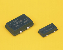
SG-615
Product competition intensified along with the expansion of the market for consumer electronics and portable information devices such as cell phones and VTRs. This led many manufacturers to fiercely compete to plan and develop smaller, lighter, and more power-efficient products to improve usability. Seeing this situation unfold and needing to quickly respond to the demand for shorter product development times, we began developing a crystal oscillator equipped with an Epson semiconductor chip that could be programmed to output a desired frequency.The result was the SG-8000 series of new crystal oscillators based on a unique new concept. Using phase locked loop (PLL) and programmable read only memory (PROM) technology, we enabled one to select and write the required oscillation frequency, output conditions, and drive voltage to an assembled oscillator using a dedicated writer.
Oscillators in the SG-8000 series could by programmed to output approximately 30,000 different frequencies. They could cover about 80% of the standard frequencies used in the market, making it possible for end-product manufacturers to use them in multiple different products simply by selecting the frequency in the program when making development prototypes. They also allowed even small volume orders to be accommodated. On top of that, the time from order receipt to delivery was reduced to one-third of the time required for conventional products. This eliminated the need to stock crystal oscillators by function and frequency, even for mass-produced products, which in turn reduced inventory and forecast order risks. - 2005
-
Epson Toyocom formed by merging Seiko Epson's and Toyocom's crystal device businesses
Seiko Epson customers were in the watch and consumer electronics Applications. Toyo Communication Equipment, on the other hand, specialized in telecommunications equipment and industrial electronic equipment. Seiko Epson excelled in photolithography and microfabrication technology, while Toyocom had expertise in the basic theory of crystal devices. The crystal device operations of the two companies were merged to form a new company, Epson Toyocom Corporation.
Around the same time, the FA-128 AT-cut crystal unit was exhibited at CEATEC JAPAN 2005. Panels showed the photo-AT fabrication process, and the devices displayed were tiny, with external dimensions of 2.0 mm x 1.6 mm x 0.5 mm. The FA-128, far smaller than its predecessor thanks to a photolithography process, made a huge impact on visitors. -
Quartz gyroscopic sensors adopted for image stabilization applications in digital SLR cameras
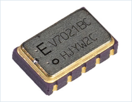 Gyroscopic sensors are responsible for accurately detecting changes in angular rate, but they needed to be smaller and more stable to meet the demand for equipment with greater functionality and precision. Epson gyroscopic sensors employ quartz, an extremely stable material whose characteristics are innately resistant to change over a range of temperatures. Moreover, Epson proprietary photolithography process produces among the world's smallest gyroscopic sensors that, despite their diminutive size, boast outstanding stability and precision.
The secret to their performance is a unique hammerhead (double-T) structure realized by using photolithography. Their small size and high sensitivity belie their low noise and high stability. In short, our gyroscopic sensors can be installed in small devices, where they provide stable accuracy even in harsh temperature environments. The recognized performance of our quartz gyroscopic sensors has earned them a place in image stabilization in digital SLR cameras, and they continue to contribute to accurate detection of angular velocity changes in car navigation systems, vehicle safety systems, and other applications. - 2009
- Epson Toyocom becomes a wholly owned subsidiary of Seiko Epson.
- 2011
-
Development of one of the world's smallest*1 IMUs*2 with among the lowest power consumption
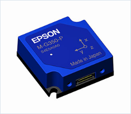 Initially, inertial measurement units (IMUs) were mostly embedded in specialized equipment for aerospace applications and other uses that require highly accurate, stable measurement of inertial measurement. Later, however, IMUs developed for industrial applications began finding their way into a variety of products. What the new and expanding industrial Applications wanted were IMUs that offered greater accuracy and stability yet were also smaller and drew less power, as these attributes would make them easier to build into products.
Epson, the rare company with both a semiconductor and a crystal device business, took an original approach to developing IMUs. We first developed quartz gyroscopic (angular rate) sensors*3 by capitalizing on our unique technology to fabricate micro-electromechanical systems (MEMS) from quartz, a material known for its excellent frequency stability and high precision. We then combined these gyroscopic sensors with semiconductor technology and expertise accumulated in the development of GPS modules and other position information devices to complete the IMU.With outstanding precision and stability measurement capabilities, the IMU was able to accurately sense inertial motion, from the slightest of tilts to large movements. The small form factor, light weight, and low power consumption made it easier to embed into products than earlier IMUs, giving product engineers more design freedom. Engineers were able to easily embed this IMU into a wide variety of industrial systems used to analyze and control inertial motion, control moving objects control vibration stability and control navigation.
*1 Compared to other small IMUs that had been used in industrial applications (per Epson research conducted in May 2011)
*2 An IMU is a device that is used for sensing inertial motion. It is comprised of triaxial angular rate sensors and triaxial accelerometers. IMUs are primarily used to measure and control the behavior of moving objects.
*3 Gyroscopic sensors measure the rotation angle (angular rate) of an object per unit of time around a sensing axis. - 2012
- Certain operations of Epson Toyocom are split off and absorbed by Epson.
- After 2020
- Advances in IoT, 5G, automated driving, etc., and the growing severity of societal issues

Epson Crystal Devices will continue to contribute to the realization of a smart society and contribute solutions to societal issues.


