Basic Knowledge of Crystal Unit
Crystal unit
1. Vibration Modes and Orientation Angles
Regarding the vibration mode of the AT cut, the orientation angle at which the primary coefficient of the frequency temperature characteristics near room temperature reaches zero is indicated in Fig.1
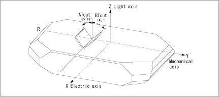
Fig.1 Orientation angle in Z plate artificial crystals
And the mode of thickness shear vibration is shown virtually in Fig.2

Fig.2 Thickness shear vibration
Regarding generally used AT cut crystals, their frequency ranges and frequency coefficients (the relationship between the thickness of crystal plate and oscillation frequency) are shown in Table 1.
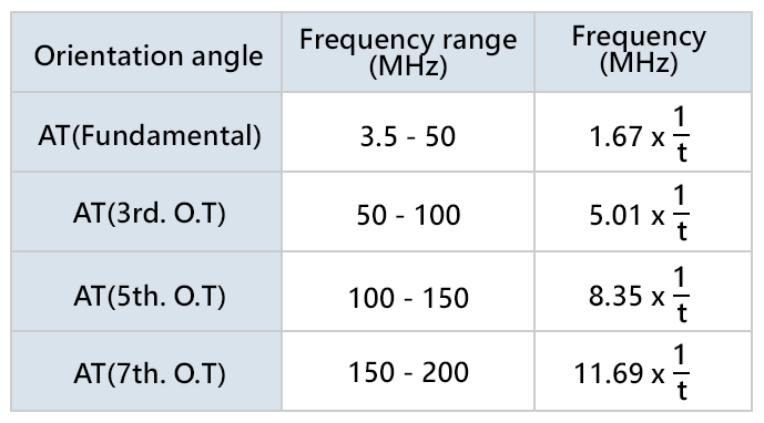
Table 1 Relationship between orientation angle and frequency
2. Frequency-temperature characteristics
The frequency-temperature characteristics of a crystal are categorized into two types according to its shape of curve. One is a tertiary curve and the other is a quadratic curve. The typical frequency-temperature characteristics of AT cut are shown in Fig.3 and Fig.4, respectively. AT cut crystal units are most widely used because they produce smaller frequency changes in response to temperature changes in the room temperature range.
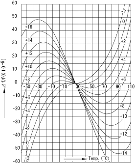
Fig.3 Example of AT cut frequency stability
3. Equivalent circuit and various constants
The equivalent circuit of quartz crystal near the resonance frequency is represented by the arrangements shown in Fig.5.
R1:Series Resistance
L1: Motional Inductance
C1: Motional Capacitance
C0: Shunt Capacitance
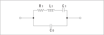
Fig.5 Equivalent circuit of quartz crystals
The admittance locus diagram of a crystal unit near its oscillation frequency and the equivalent circuit of a crystal unit are shown in Fig.6.This chart and figure show the configuration of the equivalent circuit under various circuit conditions and the relationship between oscillation frequency and resistance, etc.Here, we can find the following relationships among the various constants
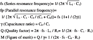
Fig.6 Admittance locus diagram
Oscillation circuit with quartz crystal
1. Typical Oscillation Circuit (Fundamental oscillation mode)
A typical oscillation circuit diagram is shown in Fig.7.
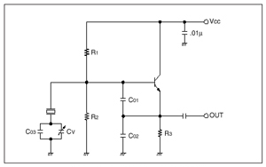
Fig.7 Typical oscillation circuit in fundamental vibration mode
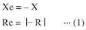
When the oscillation mode is in a steady state, the relations among the reactance of crystal unit Xe, circuit reactance -X, impedance of crystal Re and circuit impedance -R are as follows:
And the simplified oscillation circuit in a steady state is shown in Fig.8.
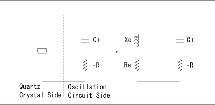
Fig.8 Equivalent oscillation circuit of parallel resonance oscillation circuit
To obtain secure oscillation of the circuit, the negative resistance of the circuit must satisfy the following equation : -R | > Re.
Taking the circuit in Fig.7 as an example, the negative resistance of the circuit is shown as follows:
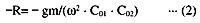
Here,
gm = Mutual conductance of a transistor at the oscillation stage
ω( = 2π / f ) = Oscillation angle frequency
2. Load capacitance and oscillation frequency
Given that
Series resonance frequency = fr
Equivalent Series Capacitance = C1
Parallel Capacitance = C0
Resonance Frequency (With Load Capacitance CL) = fL
and fL - fr = deltaf
then,
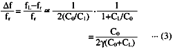
The above equation is induced.
The load capacitance can be regarded as the series capacitance of C01,
C02 and C03 + CV, as shown in Fig.7., including stray capacitances of transistors and circuit patterns.
Therefore, the load capacitance CL is given by the following equation.
The "pulling range", the frequency variation range when the load capacitance of the oscillation circuit can be altered from CL1 to CL2, is expressed as,
If the equivalent series capacitance C1, parallel capacitance C0, and the above CL1 and CL2 are given, the frequency variation range can be induced from the above equation. The "pulling Sensitivity", the sensitivity of an element near the load capacitance (CL), is given by the following equation.
The resonance frequency vs. load capacitance characteristics are shown in Fig. 9. The result of calculating the above equations (3), (5), (6)
under the given conditions of C1 = 16fF, C0 = 3.5pF, CL = 30pF, CL1 = 27pF, and CL2 = 33pF.
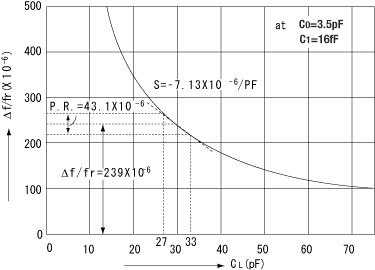
Fig.9 Frequency vs. load capacitance
By applying this phenomenon, the output frequency of the oscillationcircuit can be trimmed to the nominal frequency, by adjusting a variable trimmer capacitor to offset the deviation due to production deviation of the crystal unit and the deviation of components in the oscillation circuit.
Although a reduction in the load capacitance (CL) in Equation (6) will increase the device sensitivity, it will also, conversely, decrease the stability.
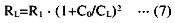
Please note that a reduction in the load capacitance will increase the difficulty in starting oscillation because the effective resistance of the crystal unit will increase, as shown in equation (7).
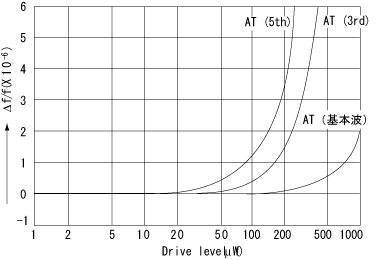
3. Drive level of crystal oscillator
In order to ensure the stable oscillation of the crystal oscillator, a certain degree of drive power must be applied. Fig.13 shows how the frequency varies with the drive level, the amount of the frequency shift increasing as the drive level increases.
Applying a high drive power (approx. 50mW) to a crystal unit will cause damage to it. For use in a normal oscillation circuit,
the preferred drive power is 0.1 mW or less (max. 0.5 mW).
4. The following points must be considered when designing a PCB pattern.
The pattern length from the oscillation stage to the crystal unit shall be the minimum in order to keep the stray capacitance of the oscillation loop to a minimum.
When putting other components and wiring patterns over the oscillation loop, the increase of stray capacity shall be kept to a minimum.