For customers using NXP Semiconductors "LPC1xxxx series"
We are pleased to introduce you to our crystal unit.
Items to Confirm (designing of oscillation circuit)
Please note: to design oscillation circuit, you need to confirm the electronic characteristics as follows:
Oscillation allowance and Negative resistance (-R):
You need to confirm oscillation capability.
We recommend the condition: (-R) / ESR > 5
* -R: Negative resistance, ESR: Equivalent Series Resistance
Drive Level:
You need to confirm if oscillation is stable, and if the drive level is within the specification.
Load Capacitance:
Load capacitance affects frequency stability, oscillation allowance, negative resistance, and start-up time of oscillation.
In addition the load capacitance is determinative factor of crystal unit's load capacitance (CL value) directly.
For details of each characteristic, please refer to the PDF file.
Precautions for Oscillation Circuit DesignSelection Guidance for crystal unit
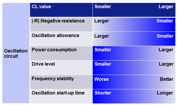
When Customer selects crystal unit, load capacitance (CL value) is an important factor of the selection.
For instance, crystal with small CL(7.0 pF) makes larger oscillation allowance, smaller current consumption and worse frequency stability,
like below table. Oppositely, crystal with large CL(12.5 pF) makes smaller oscillation allowance, larger current consumption and better frequency stability.
Please select it in consideration of these characteristics.
Epson Crystal Product Lineups
| Product | Size [mm] | Applications | Images |
|---|---|---|---|
| MC-146 | 7.0 x 1.5 x 1.4 | DSC, Consumer equipment,Radio equipment, Blood pressure meter,Blood-sugar monitor, Security systems |  |
| FC-135 FC-135R |
3.2 x 1.5 x 0.9 | PMP, DSC, Portable equipment |  |
| FA-238 FA-238V |
3.2 x 2.5 x 0.7 | -Mobile phone,Bluetooth,W-LAN -ISM band,Clock for MPU |
 |
| FA-20H | 2.5 x 2.0 x 0.55 |  |
Oscillation Circuit and Selection Guidance of Crystal Unit for LPCxxxx micro controller
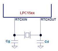
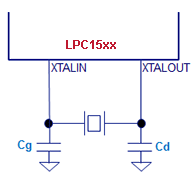
LPC15xx series
1) 32 kHz
| Product Name | Frequency [Hz] |
CL*1 [pF] |
Product Code*2 | External Parts*3 | Drive Level [µW] |
Package Size WxDxH [mm] |
|
|---|---|---|---|---|---|---|---|
| Cg [pF] |
Cd [pF] |
||||||
| FC-135 | 32.768k | 12.5 | Q13FC13500004** | 22 | 18 | 0.11 | 3.2 x 1.5 x 0.9 |
| MC-146 | 32.768k | 12.5 | Q13MC14620002** | 22 | 18 | 0.13 | 7.0 x 1.5 x 1.4 |
Notes:
Please follow these recommendations and don't use any external capacitors for Cd and Cg below the recommended values.
2) 12 MHz
| Product Name | Frequency [Hz] |
CL*1 [pF] |
Product Code*2 | External Parts*3 | Drive Level [µW] |
Package Size WxDxH [mm] |
|
|---|---|---|---|---|---|---|---|
| Cg [pF] |
Cd [pF] |
||||||
| FA-238V | 12M | 10 | Q22FA23V00019** | 7 | 7 | 37 | 3.2 x 2.5 x 0.7 |
| FA-238V | 12M | 12 | Q22FA23V00007** | 10 | 10 | 49 | 3.2 x 2.5 x 0.7 |
| FA-20H | 12M | 10 | Q24FA20H00152** | 7 | 7 | 69 | 2.5 x 2.0 x 0.55 |
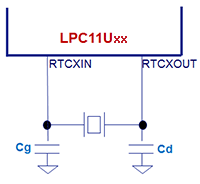
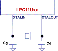
LPC11Uxx series
1) 32 kHz
| Product Name | Frequency [Hz] |
CL*1 [pF] |
Product Code*2 | External Parts*3 | Drive Level [µW] |
Package Size WxDxH [mm] |
|
|---|---|---|---|---|---|---|---|
| Cg [pF] |
Cd [pF] |
||||||
| FC-135 | 32.768k | 12.5 | Q13FC13500004** | 22 | 18 | 0.09 | 3.2 x 1.5 x 0.9 |
| MC-146 | 32.768k | 12.5 | Q13MC14620002** | 18 | 18 | 0.10 | 7.0 x 1.5 x 1.4 |
Notes:
Please follow these recommendations and don't use any external capacitors for Cd and Cg below the recommended values.
2) 12 MHz
| Product Name | Frequency [Hz] |
CL*1 [pF] |
Product Code*2 | External Parts*3 | Drive Level [µW] |
Package Size WxDxH [mm] |
|
|---|---|---|---|---|---|---|---|
| Cg [pF] |
Cd [pF] |
||||||
| FA-238V | 12M | 10 | Q22FA23V00019** | 7 | 7 | 34 | 3.2 x 2.5 x 0.7 |
| FA-238V | 12M | 12 | Q22FA23V00007** | 10 | 10 | 43 | 3.2 x 2.5 x 0.7 |
| FA-20H | 12M | 10 | Q24FA20H00152** | 7 | 7 | 59 | 2.5 x 2.0 x 0.55 |
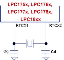
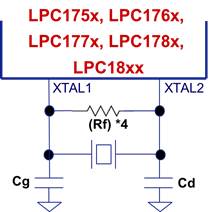
LPC175x, LPC176x, LPC177x, LPC178x, LPC18xx series
1) 32 kHz
| Product Name | Frequency [Hz] |
CL*1 [pF] |
Product Code*2 | External Parts*3 | Drive Level [µW] |
Package Size WxDxH [mm] |
|
|---|---|---|---|---|---|---|---|
| Cg [pF] |
Cd [pF] |
||||||
| FC-135 | 32.768k | 12.5 | Q13FC13500004** | 22 | 22 | 0.094 | 3.2 x 1.5 x 0.9 |
| MC-146 | 32.768k | 12.5 | Q13MC14620002** | 22 | 18 | 0.005 | 7.0 x 1.5 x 1.4 |
Notes:
Please follow these recommendations and don't use any external capacitors for Cd and Cg below the recommended values.
2) 12 MHz
| Product Name | Frequency [Hz] |
CL*1 [pF] |
Product Code*2 | External Parts*3 | Drive Level [µW] |
Package Size WxDxH [mm] |
||
|---|---|---|---|---|---|---|---|---|
| Cg [pF] |
Cd [pF] |
Rf *4 [Ω] |
||||||
| FA-238V | 12M | 10 | Q22FA23V00019** | 10 | 10 | 1M | 45 | 3.2 x 2.5 x 0.7 |
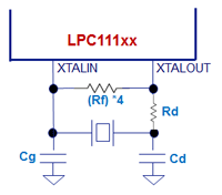
LPC111x series
1) 12 MHz, 16 MHz
| Product Name | Frequency [Hz] |
CL*1 [pF] |
Product Code*2 | External Parts*3 | Drive Level [µW] |
Package Size WxDxH [mm] |
|||
|---|---|---|---|---|---|---|---|---|---|
| Cg [pF] |
Cd [pF] |
Rf *4 [Ω] |
Rd [Ω] |
||||||
| FA-238V | 12M | 10 | Q22FA23V00019** | 12 | 12 | 1M | - | 44 | 3.2 x 2.5 x 0.7 |
| FA-238 | 16M | 10 | Q22FA23800421** | 18 | 15 | 1M | 470 | 72 | 3.2 x 2.5 x 0.7 |
Notes:*
*1. Load capacitance.
*2. Two digits of the product code is packing specification,please refer here for the detail.
*3. Above recommendations are based on actual evaluation results and intended to support users in picking the right components. And the results are only according to the sample set that received from our customers, so it is not including the dispersion trend of IC and the external parts.
As the actual board layout and choice of external components influences the best suitable crystal load capacitance, We do not assume any responsibility and grant warranty for above recommendations. Users design must be verified and decided by own and individual evaluation.
*4. Please evaluate a crystal oscillator without an external feedback resistor Rf if you need. It is possible that a crystal oscillator works without it because LCP1xxx has an internal feedback resistor Rf in the MHz oscillator.
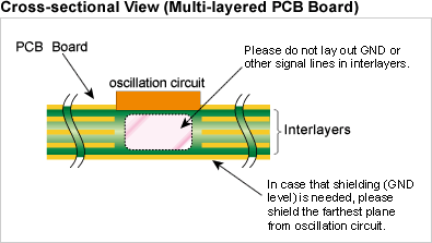
Precautions for designing of PCB Board
Layout of pins, Crystal unit, Capacitor and Resistor
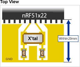
- Please lay out crystal unit, capacitor and resistor near LPC1xxxx as far as possible.
- The length of signal patterns in oscillation circuit should be as short as possible, and do not cross other signal lines.
For 32 kHz Crystal unit
GND Line Pattern and Interconnection of PCB
- Please lay out GND line pattern under crystal unit.
- In case of multi-layered PCB board, do not lay out other signal lines under crystal unit.